


Description
Optical Defect InspectionConfiguration
No ConfigurationOEM Model Description
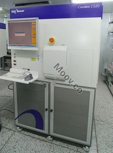
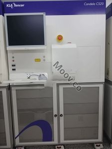
The Candela CS20 system measures surface reflectivity and topography for automatic defect detection and classification. It uses scatterometry, ellipsometry, reflectometry, and topographical analysis to inspect wafer surfaces for defects and film thickness uniformity. It is designed for inspection of transparent materials such as sapphire and GaN and can detect a wide variety of defects. It is suitable for use in the production of High Brightness Light Emitting Diodes (HBLEDs), High-Power RF Devices, and Coated Glass (CMOS imagers, LCoS chips, etc.).Documents
No documents

Verified
CATEGORY
Defect Inspection
Last Verified: Over 60 days ago
Key Item Details
Condition:
Used
Operational Status:
Unknown
Product ID:
115117
Wafer Sizes:
6"/150mm
Vintage:
2006
Logistics Support
Available
Transaction Insured by Moov
Available
Refurbishment Services
Available
Similar Listings
View All


KLA
CANDELA CS20
CATEGORY
Defect Inspection
Last Verified: Over 60 days ago


Key Item Details
Condition:
Used
Operational Status:
Unknown
Product ID:
115117
Wafer Sizes:
6"/150mm
Vintage:
2006
Logistics Support
Available
Transaction Insured by Moov
Available
Refurbishment Services
Available
Description
Optical Defect InspectionConfiguration
No ConfigurationOEM Model Description
The Candela CS20 system measures surface reflectivity and topography for automatic defect detection and classification. It uses scatterometry, ellipsometry, reflectometry, and topographical analysis to inspect wafer surfaces for defects and film thickness uniformity. It is designed for inspection of transparent materials such as sapphire and GaN and can detect a wide variety of defects. It is suitable for use in the production of High Brightness Light Emitting Diodes (HBLEDs), High-Power RF Devices, and Coated Glass (CMOS imagers, LCoS chips, etc.).Documents
No documents