


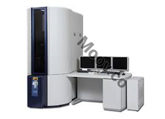
Description
Cs-corrected scanning transmission electron microscope (STEM)Configuration
Camera / detectors: Gatan CCD Orius SC 1000 W HAADF, MAADF, DF, BF and SE detectors EDX ENFINA / EELS Key features: Acceleration voltages: 80, 120 and 200 kV Cold field emitter Cs-corrector Resolution: 0.105 nm Holders: 360° Tomography holder Heating holder 20-800 °C Single and double tilt holder Cryo-Holder (LN2)OEM Model Description
The HD-2700 is an 80-200 kV field-emission-gun scanning transmission electron microscope (STEM) with secondary electron (SE) imaging capability. Bulk and surface structures of a specimen can be imaged simultaneously. With the option for a probe-forming aberration corrector, ultra-high resolution can be achieved for both STEM and SE imaging. The Hitachi corrector minimizes the user's effort in doing aberration correction. Large solid-angle EDS* and atomic-spatial-resolution EDS* and EELS spectrum imaging* are enabled.Documents
No documents


HITACHI
HD-2700
CATEGORY
SEM / FIB
Last Verified: 3 days ago


Key Item Details
Condition:
Used
Operational Status:
Unknown
Product ID:
163170
Wafer Sizes:
Unknown
Vintage:
Unknown
Logistics Support
Available
Transaction Insured by Moov
Available
Refurbishment Services
Available
Description
Cs-corrected scanning transmission electron microscope (STEM)Configuration
Camera / detectors: Gatan CCD Orius SC 1000 W HAADF, MAADF, DF, BF and SE detectors EDX ENFINA / EELS Key features: Acceleration voltages: 80, 120 and 200 kV Cold field emitter Cs-corrector Resolution: 0.105 nm Holders: 360° Tomography holder Heating holder 20-800 °C Single and double tilt holder Cryo-Holder (LN2)OEM Model Description
The HD-2700 is an 80-200 kV field-emission-gun scanning transmission electron microscope (STEM) with secondary electron (SE) imaging capability. Bulk and surface structures of a specimen can be imaged simultaneously. With the option for a probe-forming aberration corrector, ultra-high resolution can be achieved for both STEM and SE imaging. The Hitachi corrector minimizes the user's effort in doing aberration correction. Large solid-angle EDS* and atomic-spatial-resolution EDS* and EELS spectrum imaging* are enabled.Documents
No documents