


Description
SystemConfiguration
Main process METAL Sub Process PVD Materials Ti, TIN, TAN, AL Operating system Window HDD: removed Hardware Composition EFEM: 1 Transfer Module: 1 Process Chambers: 9 Utility AC Rack: 3 Generator Rack: 5 Accessory Box: 1 CVCF: 1 EFEM Intake: 1 EFEM Side Panel: 2 Compressor: 1 DI Max: 2 Monitor Stand: 2 Process Modules Chamber 1: PVD Ti Chamber 2: PVD TiN Chamber 3: PVD Al Chamber 4: PVD Al Chamber 5: PVD TaN Chamber C: Preclean Chamber D: PrecleanOEM Model Description
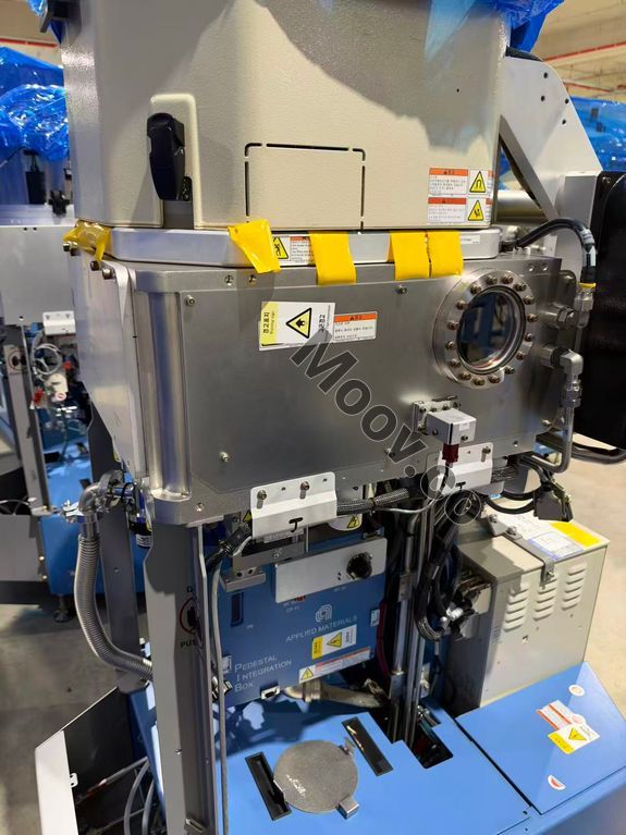
The Applied Materials ENDURA II is a highly advanced platform used in the semiconductor industry for physical vapor deposition (PVD) processes. It is designed to deposit thin films of various materials onto semiconductor wafers with exceptional precision and uniformity.Documents
No documents

CATEGORY
PVD / Sputtering
Last Verified: Today
Key Item Details
Condition:
Used
Operational Status:
Unknown
Product ID:
164853
Wafer Sizes:
12"/300mm
Vintage:
2006
Logistics Support
Available
Transaction Insured by Moov
Available
Refurbishment Services
Available
Similar Listings
View All


APPLIED MATERIALS (AMAT)
ENDURA II
CATEGORY
PVD / Sputtering
Last Verified: Today


Key Item Details
Condition:
Used
Operational Status:
Unknown
Product ID:
164853
Wafer Sizes:
12"/300mm
Vintage:
2006
Logistics Support
Available
Transaction Insured by Moov
Available
Refurbishment Services
Available
Description
SystemConfiguration
Main process METAL Sub Process PVD Materials Ti, TIN, TAN, AL Operating system Window HDD: removed Hardware Composition EFEM: 1 Transfer Module: 1 Process Chambers: 9 Utility AC Rack: 3 Generator Rack: 5 Accessory Box: 1 CVCF: 1 EFEM Intake: 1 EFEM Side Panel: 2 Compressor: 1 DI Max: 2 Monitor Stand: 2 Process Modules Chamber 1: PVD Ti Chamber 2: PVD TiN Chamber 3: PVD Al Chamber 4: PVD Al Chamber 5: PVD TaN Chamber C: Preclean Chamber D: PrecleanOEM Model Description
The Applied Materials ENDURA II is a highly advanced platform used in the semiconductor industry for physical vapor deposition (PVD) processes. It is designed to deposit thin films of various materials onto semiconductor wafers with exceptional precision and uniformity.Documents
No documents