


Description
No descriptionConfiguration
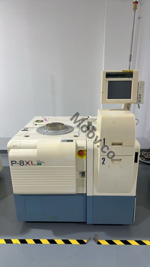
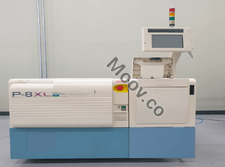
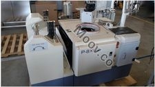
Description Technical parameters 1 Hardware Chuck: Material: Gold-plated Chuck Size: Compatible with 6-inch and 8-inch screens Wafer delivery system: Mapping module: Automatic image scanning Arm: Compatible with 6-inch and 8-inch wafer transmission Film transfer method: robotic arm (width) Index: ≥350um Wafer transfer: Supports transfer up to 200µm Wafer alignment system: Automatic alignment, centering, and positioning; supports target die mode Pre-alignment module: Equipped with a pre-alignment stage, supporting 0~360° wafer edge finding. Pin ModuleL Low magnification lens High magnification lens Manual/Automatic Pin Alignment Module Needle cleaning module: Automatic needle clearing module Needle cleaning platform height calibration module (CCD) Disassembled needle cleaning platform Multi-Site module: Supports multi-site testing FTP networking: Supports automatic uploading of mappings via FTP server Communication module: GPIB communication PC: monitor Cardholder: Supports switching between round and square cards. EMOModule: Equipped with an EMO button 2 Software Wafer Alignment: Supports wafer edge finding function, with adjustable on/off angle and orientation, supporting 0~360°. Needle Alignment: Supports automatic needle setting function, capable of setting needles at high and low magnification levels. Muti- siteAutomatic needle setting Needle Cleaning: Supports automatic needle clearing function, can be followed X,Y Directional movement method for needle clearing. Measurable needle cleaning platform height and flatness Multi-SiteTest: supportMulti-Site Test Wafer ID Reading: Supports manual Wafer ID input; simply enter a serial number from 1 to 25. Wafer Map Edit: supply DEVICE COMMAND The software allows users to delete and modify MAP files and supports file import and export functions. Fail Die retest function: Supports retesting by specifying a BIN or retesting all fail dies. Timeout alarm function: Supports communication timeout alarm Continuous failure alarm function: Supports continuous failure alarms Mapping maximum number of test dies: Maximum capacity of 170,000 diesOEM Model Description
The P-8XL Prober is a market innovation in the wafer probing industry by TEL. It offers superior accuracy, reliability, efficiency, and integration for the test cell through its features such as on-axis alignment, optical wafer profiling, and direct test head docking. The P-8XL is equipped with a fully interactive LCD Touch Panel Screen and TEL’s advanced On-Axis Alignment System, delivering guaranteed pin-to-pad accuracy. It also offers a range of features to overcome probe floor barriers, including Direct Coupling Test Interfaces, Automatic Probe Card Changers, Clean Air Management Systems, Temperature Controlled Chucks, and many others. With its advanced capabilities, the P-8XL is ready to meet the demands of future device complexity and measurement precision.Documents
No documents

Verified
CATEGORY
Probers
Last Verified: Over 30 days ago
Key Item Details
Condition:
Used
Operational Status:
Unknown
Product ID:
148222
Wafer Sizes:
Unknown
Vintage:
1999
Logistics Support
Available
Transaction Insured by Moov
Available
Refurbishment Services
Available
Similar Listings
View All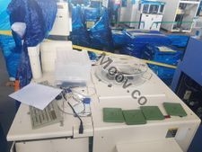


TEL / TOKYO ELECTRON
P-8XL
CATEGORY
Probers
Last Verified: Over 30 days ago


Key Item Details
Condition:
Used
Operational Status:
Unknown
Product ID:
148222
Wafer Sizes:
Unknown
Vintage:
1999
Logistics Support
Available
Transaction Insured by Moov
Available
Refurbishment Services
Available
Description
No descriptionConfiguration
Description Technical parameters 1 Hardware Chuck: Material: Gold-plated Chuck Size: Compatible with 6-inch and 8-inch screens Wafer delivery system: Mapping module: Automatic image scanning Arm: Compatible with 6-inch and 8-inch wafer transmission Film transfer method: robotic arm (width) Index: ≥350um Wafer transfer: Supports transfer up to 200µm Wafer alignment system: Automatic alignment, centering, and positioning; supports target die mode Pre-alignment module: Equipped with a pre-alignment stage, supporting 0~360° wafer edge finding. Pin ModuleL Low magnification lens High magnification lens Manual/Automatic Pin Alignment Module Needle cleaning module: Automatic needle clearing module Needle cleaning platform height calibration module (CCD) Disassembled needle cleaning platform Multi-Site module: Supports multi-site testing FTP networking: Supports automatic uploading of mappings via FTP server Communication module: GPIB communication PC: monitor Cardholder: Supports switching between round and square cards. EMOModule: Equipped with an EMO button 2 Software Wafer Alignment: Supports wafer edge finding function, with adjustable on/off angle and orientation, supporting 0~360°. Needle Alignment: Supports automatic needle setting function, capable of setting needles at high and low magnification levels. Muti- siteAutomatic needle setting Needle Cleaning: Supports automatic needle clearing function, can be followed X,Y Directional movement method for needle clearing. Measurable needle cleaning platform height and flatness Multi-SiteTest: supportMulti-Site Test Wafer ID Reading: Supports manual Wafer ID input; simply enter a serial number from 1 to 25. Wafer Map Edit: supply DEVICE COMMAND The software allows users to delete and modify MAP files and supports file import and export functions. Fail Die retest function: Supports retesting by specifying a BIN or retesting all fail dies. Timeout alarm function: Supports communication timeout alarm Continuous failure alarm function: Supports continuous failure alarms Mapping maximum number of test dies: Maximum capacity of 170,000 diesOEM Model Description
The P-8XL Prober is a market innovation in the wafer probing industry by TEL. It offers superior accuracy, reliability, efficiency, and integration for the test cell through its features such as on-axis alignment, optical wafer profiling, and direct test head docking. The P-8XL is equipped with a fully interactive LCD Touch Panel Screen and TEL’s advanced On-Axis Alignment System, delivering guaranteed pin-to-pad accuracy. It also offers a range of features to overcome probe floor barriers, including Direct Coupling Test Interfaces, Automatic Probe Card Changers, Clean Air Management Systems, Temperature Controlled Chucks, and many others. With its advanced capabilities, the P-8XL is ready to meet the demands of future device complexity and measurement precision.Documents
No documents