5130
Category
MetrologyOverview
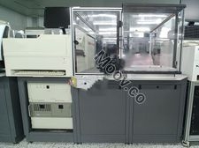
The SSM 5130 is a fully automatic mapping system that provides a variety of electrical characterization measurements for non-patterned wafers used in epitaxial silicon production and front-end semiconductor processing. Wafers are robotically loaded onto the mapping stage from a cassette or opened FOUP, and the test wafer moves to each site specified in a pre-programmed map as electrical characterization tests are made. The system stores test data and reports it in a variety of formats. The SSM 5130 eliminates the need for costly metal and poly deposition processes by using a pneumatically controlled, non-damaging probe design and a top-side mercury contact. With separate probe and chuck vacuum lines, the system features an extremely stable contact area and uses only a small quantity of mercury to make highly repeatable measurements for process development and process monitoring applications. Typical applications of the SSM 5130 include EPI resistivity, low-k dielectric constant, and oxide integrity. The SSM 5130 can handle wafer diameters from 200 mm to 300 mm, and offers single-site and multiple-site maps. Automatic face-up loading prevents wafer damage, and precision pressure regulators are used for Hg contact. The PROCAP software provides a full suite of measurements.
Active Listings
1
Services
Inspection, Insurance, Appraisal, Logistics