

Description
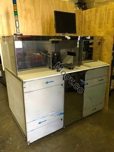
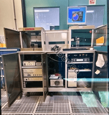
Non-contact CV/IV Measurement SystemConfiguration
. Automatic robotic wafer handling . Single open-cassette wafer loading station . Measurement of dielectric and interface properties on monitor wafer - Dielectric Capacitance (CD) and Thickness (EOT) - Dielectric Leakage Current (I-V) - Flatband Voltage (Vfb) - Interface Trap Density (Dit) - Interface Trapped Charge (Qit) - Semiconductor Surface Barrier (Vsb) - Oxide Total Charge (Qtot) - Mobile Ionic Charge (Qm), among others . Suitable for measurement on: - Semiconductor wafers (e.g. Si, SiGe, InGaAs, SiC, GaN) with high-k and low-k dielectric films (e.g. SiO2, SiNx, Al2O3, HfO2 ;..)OEM Model Description
The SEMILAB FAAST 230 is a non-contact, fast in-line monitoring system designed to detect heavy metal contamination, including sub 108 atoms/cm-3 Fe detection, in a medium to high-volume manufacturing environment. It features automated wafer handling, with options for SMIF/FOUP Loadport/Versaport, and can perform full wafer FAST mapping of diffusion length, Iron, and other recombination centers. The system is configurable for 100 mm to 300 mm wafers and is compatible with other Semilab SDI FAaST tool measurement technologies. Additional options include a minienvironment, wafer edge-grip handling, wafer flipper for automatic backsurface measurement, and more.Documents
No documents
SEMILAB
FAAST 230

Verified
CATEGORY
Metrology
Last Verified: 24 days ago
Key Item Details
Condition:
Used
Operational Status:
Unknown
Product ID:
102007
Wafer Sizes:
8"/200mm
Vintage:
Unknown
Have Additional Questions?
Logistics Support
Available
Money Back Guarantee
Available
Transaction Insured by Moov
Available
Refurbishment Services
Available
Similar Listings
View All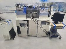

SEMILAB
FAAST 230
CATEGORY
Metrology
Last Verified: 24 days ago


Key Item Details
Condition:
Used
Operational Status:
Unknown
Product ID:
102007
Wafer Sizes:
8"/200mm
Vintage:
Unknown
Logistics Support
Available
Money Back Guarantee
Available
Transaction Insured by Moov
Available
Refurbishment Services
Available
Description
Non-contact CV/IV Measurement SystemConfiguration
. Automatic robotic wafer handling . Single open-cassette wafer loading station . Measurement of dielectric and interface properties on monitor wafer - Dielectric Capacitance (CD) and Thickness (EOT) - Dielectric Leakage Current (I-V) - Flatband Voltage (Vfb) - Interface Trap Density (Dit) - Interface Trapped Charge (Qit) - Semiconductor Surface Barrier (Vsb) - Oxide Total Charge (Qtot) - Mobile Ionic Charge (Qm), among others . Suitable for measurement on: - Semiconductor wafers (e.g. Si, SiGe, InGaAs, SiC, GaN) with high-k and low-k dielectric films (e.g. SiO2, SiNx, Al2O3, HfO2 ;..)OEM Model Description
The SEMILAB FAAST 230 is a non-contact, fast in-line monitoring system designed to detect heavy metal contamination, including sub 108 atoms/cm-3 Fe detection, in a medium to high-volume manufacturing environment. It features automated wafer handling, with options for SMIF/FOUP Loadport/Versaport, and can perform full wafer FAST mapping of diffusion length, Iron, and other recombination centers. The system is configurable for 100 mm to 300 mm wafers and is compatible with other Semilab SDI FAaST tool measurement technologies. Additional options include a minienvironment, wafer edge-grip handling, wafer flipper for automatic backsurface measurement, and more.Documents
No documents