


Description
No descriptionConfiguration
No ConfigurationOEM Model Description
The NOVELLUS CONCEPT TWO is a modular, integrated production system that is capable of depositing both dielectric and conductive metal layers by combining one or more processing chambers around a common, automated robotic wafer handler. It was introduced in November 1991.Documents
No documents

CATEGORY
CVD
Last Verified: Over 60 days ago
Key Item Details
Condition:
Used
Operational Status:
Unknown
Product ID:
111492
Wafer Sizes:
8"/200mm
Vintage:
2000
Logistics Support
Available
Transaction Insured by Moov
Available
Refurbishment Services
Available
Similar Listings
View All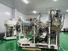


LAM RESEARCH / NOVELLUS
CONCEPT TWO "C2"
CATEGORY
CVD
Last Verified: Over 60 days ago


Key Item Details
Condition:
Used
Operational Status:
Unknown
Product ID:
111492
Wafer Sizes:
8"/200mm
Vintage:
2000
Logistics Support
Available
Transaction Insured by Moov
Available
Refurbishment Services
Available
Description
No descriptionConfiguration
No ConfigurationOEM Model Description
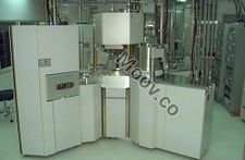
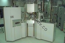
The NOVELLUS CONCEPT TWO is a modular, integrated production system that is capable of depositing both dielectric and conductive metal layers by combining one or more processing chambers around a common, automated robotic wafer handler. It was introduced in November 1991.Documents
No documents