


Description
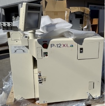
Automatic Wafer Prober Primary Function: Positions 8-inch to 12-inch wafers under a test head for automatic electrical testing of die sites Main Unit (Chassis) Marked P-12XL and labeled Fully Automatic Wafer Prober. Houses motion stages, vacuum systems, and electronic controls. The large red button is an emergency stop (EMO). Door on the front provides access to power and control electronics. Operator Interface / Display Head The upper monitor arm holds a control terminal (CRT or early LCD type). Likely used for wafer mapping, probe alignment, and test program control. Prober Chuck Assembly (Golden Circular Plate) This is the vacuum wafer chuck, designed to hold wafers (typically up to 300 mm). temperature during testing. Surrounding wiring/tubing likely routes vacuum, temperature sensors, and nitrogen purge lines. Precision Linear Stages and Motors Inside photos show Mitsubishi servo motors and Taiyo-branded alignment units, confirming closed-loop X/Y/Z motion control. The black granite base structure gives vibration stability for sub-micron positioning accuracy. Cable Chain and Vacuum/Signal Lines Heavy cable carriers route signal lines to the moving prober head. Pneumatic and vacuum lines are tied neatly, consistent with factory-grade build. Main Console / Operator Interface "Control terminal with display and keyboard for wafer mapping, alignment, and automatic stepping. Chuck Stage Assembly Precision vacuum chuck (gold/brass colored) for wafer mounting; can be temperature-controlled (–60 °C to +200 °C range on equipped systems). XY Motion Platform Dual-rail linear motion driven by high-precision Mitsubishi servo motors and ball-screw actuators for micron-level wafer positioning. Z-Axis and Theta Control Provides contact force control and rotation for aligning probe needles with wafer pads. Probe-Card Test Head Mount Upper fixture that mates with parametric or functional test systems. Cable Chain and Pneumatic Systems Guides electrical, vacuum, and air lines cleanly to the stage and chuck. Under-Frame Modules Houses stage controllers, power supplies, and pneumatic regulators. Visible labeling (e.g., “TAIYO P-12L WAF UNIT TNP-8009”) indicates original factory modules.Configuration
Wafer Size Support 200 mm (8 in) to 300 mm (12 in) Chuck Temperature Range –60 °C to +200 °C (depends on model variant) Positioning Accuracy ±1 µm X/Y Planarity / Z Accuracy ±0.5 µm typical Alignment Optical pattern recognition (auto-alignment camera optional) Operation Mode Fully automatic with wafer mapping Power Requirements 200–240 VAC ±10%, 50/60 Hz, ≈1.5–2.5 kVA Compressed Air 0.5–0.7 MPa clean dry air Dimensions / Weight ≈ W 1.2 m × D 1.1 m × H 1.4 m / ≈ 650–750 kgOEM Model Description
The P-12XL Prober is a next-generation prober developed by TEL. It builds on the success of the P-8XL and shares the same interactive LCD Touch Panel Screen and On-axis Alignment. Additionally, it incorporates a FOUP loader, increased Z force, and higher accuracy, making it capable of tackling tomorrow’s technological challenges. The P-12XL has even been featured in the Semiconductor International article “Fabrication of the First Transistors on 300mm Wafers.Documents
No documents

Verified
CATEGORY
Probers
Last Verified: Over 60 days ago
Key Item Details
Condition:
Used
Operational Status:
Unknown
Product ID:
150382
Wafer Sizes:
8"/200mm, 12"/300mm
Vintage:
Unknown
Logistics Support
Available
Transaction Insured by Moov
Available
Refurbishment Services
Available
Similar Listings
View All




TEL / TOKYO ELECTRON
P-12XL
CATEGORY
Probers
Last Verified: Over 60 days ago


Key Item Details
Condition:
Used
Operational Status:
Unknown
Product ID:
150382
Wafer Sizes:
8"/200mm, 12"/300mm
Vintage:
Unknown
Logistics Support
Available
Transaction Insured by Moov
Available
Refurbishment Services
Available
Description
Automatic Wafer Prober Primary Function: Positions 8-inch to 12-inch wafers under a test head for automatic electrical testing of die sites Main Unit (Chassis) Marked P-12XL and labeled Fully Automatic Wafer Prober. Houses motion stages, vacuum systems, and electronic controls. The large red button is an emergency stop (EMO). Door on the front provides access to power and control electronics. Operator Interface / Display Head The upper monitor arm holds a control terminal (CRT or early LCD type). Likely used for wafer mapping, probe alignment, and test program control. Prober Chuck Assembly (Golden Circular Plate) This is the vacuum wafer chuck, designed to hold wafers (typically up to 300 mm). temperature during testing. Surrounding wiring/tubing likely routes vacuum, temperature sensors, and nitrogen purge lines. Precision Linear Stages and Motors Inside photos show Mitsubishi servo motors and Taiyo-branded alignment units, confirming closed-loop X/Y/Z motion control. The black granite base structure gives vibration stability for sub-micron positioning accuracy. Cable Chain and Vacuum/Signal Lines Heavy cable carriers route signal lines to the moving prober head. Pneumatic and vacuum lines are tied neatly, consistent with factory-grade build. Main Console / Operator Interface "Control terminal with display and keyboard for wafer mapping, alignment, and automatic stepping. Chuck Stage Assembly Precision vacuum chuck (gold/brass colored) for wafer mounting; can be temperature-controlled (–60 °C to +200 °C range on equipped systems). XY Motion Platform Dual-rail linear motion driven by high-precision Mitsubishi servo motors and ball-screw actuators for micron-level wafer positioning. Z-Axis and Theta Control Provides contact force control and rotation for aligning probe needles with wafer pads. Probe-Card Test Head Mount Upper fixture that mates with parametric or functional test systems. Cable Chain and Pneumatic Systems Guides electrical, vacuum, and air lines cleanly to the stage and chuck. Under-Frame Modules Houses stage controllers, power supplies, and pneumatic regulators. Visible labeling (e.g., “TAIYO P-12L WAF UNIT TNP-8009”) indicates original factory modules.Configuration
Wafer Size Support 200 mm (8 in) to 300 mm (12 in) Chuck Temperature Range –60 °C to +200 °C (depends on model variant) Positioning Accuracy ±1 µm X/Y Planarity / Z Accuracy ±0.5 µm typical Alignment Optical pattern recognition (auto-alignment camera optional) Operation Mode Fully automatic with wafer mapping Power Requirements 200–240 VAC ±10%, 50/60 Hz, ≈1.5–2.5 kVA Compressed Air 0.5–0.7 MPa clean dry air Dimensions / Weight ≈ W 1.2 m × D 1.1 m × H 1.4 m / ≈ 650–750 kgOEM Model Description
The P-12XL Prober is a next-generation prober developed by TEL. It builds on the success of the P-8XL and shares the same interactive LCD Touch Panel Screen and On-axis Alignment. Additionally, it incorporates a FOUP loader, increased Z force, and higher accuracy, making it capable of tackling tomorrow’s technological challenges. The P-12XL has even been featured in the Semiconductor International article “Fabrication of the First Transistors on 300mm Wafers.Documents
No documents