


Description
No descriptionConfiguration
Windows System Main S/W Wafer Size 300mm SEMI Notch Facilities Power: 208 VAC, 3W N CDA: > 28.3 Nl /min, > 6.6791 kg /cm2 Vac: > 28.317 l/min, > 700 mm Hg Load port Vacuum 200mm and 300mm FIMS Computer Mouse Keyboard 3.5" FEC computerOEM Model Description
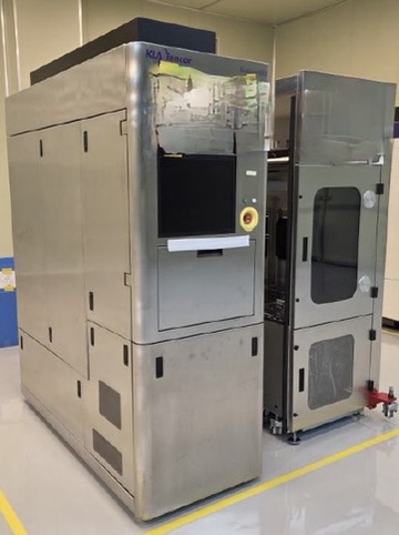
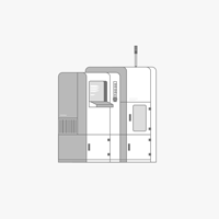
The Surfscan SP2 is an unpatterned wafer surface inspection tool that uses UV laser technology, darkfield optics, and advanced algorithms to detect defects as small as 30nm. It provides high sensitivity detection on engineered substrates and has a significant throughput increase over the prior-generation tool. It offers a single tool solution for three technology nodes and has comprehensive wafer surface inspection capabilities. It also enables faster root-cause analysis with improved coordinate accuracy and real-time defect classification capability.Documents
No documents

Verified
CATEGORY
Defect Inspection
Last Verified: Over 30 days ago
Key Item Details
Condition:
Used
Operational Status:
Unknown
Product ID:
150853
Wafer Sizes:
12"/300mm
Vintage:
2006
Logistics Support
Available
Transaction Insured by Moov
Available
Refurbishment Services
Available
Similar Listings
View All




KLA
SURFSCAN SP2
CATEGORY
Defect Inspection
Last Verified: Over 30 days ago


Key Item Details
Condition:
Used
Operational Status:
Unknown
Product ID:
150853
Wafer Sizes:
12"/300mm
Vintage:
2006
Logistics Support
Available
Transaction Insured by Moov
Available
Refurbishment Services
Available
Description
No descriptionConfiguration
Windows System Main S/W Wafer Size 300mm SEMI Notch Facilities Power: 208 VAC, 3W N CDA: > 28.3 Nl /min, > 6.6791 kg /cm2 Vac: > 28.317 l/min, > 700 mm Hg Load port Vacuum 200mm and 300mm FIMS Computer Mouse Keyboard 3.5" FEC computerOEM Model Description
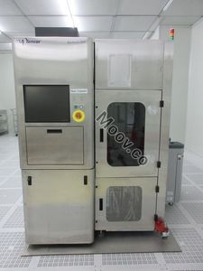
The Surfscan SP2 is an unpatterned wafer surface inspection tool that uses UV laser technology, darkfield optics, and advanced algorithms to detect defects as small as 30nm. It provides high sensitivity detection on engineered substrates and has a significant throughput increase over the prior-generation tool. It offers a single tool solution for three technology nodes and has comprehensive wafer surface inspection capabilities. It also enables faster root-cause analysis with improved coordinate accuracy and real-time defect classification capability.Documents
No documents