


Description
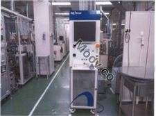
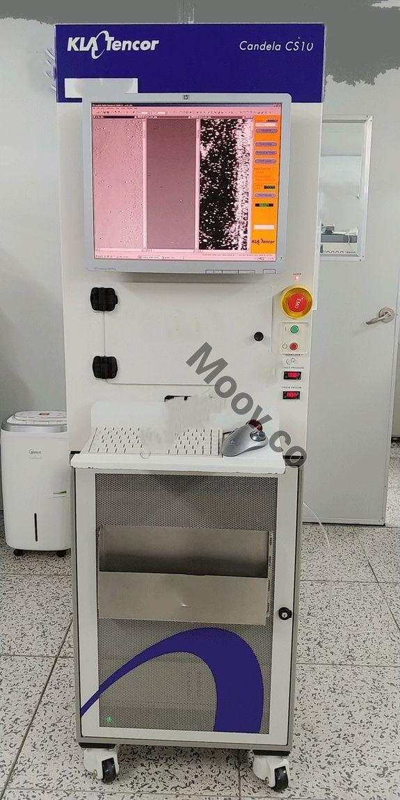
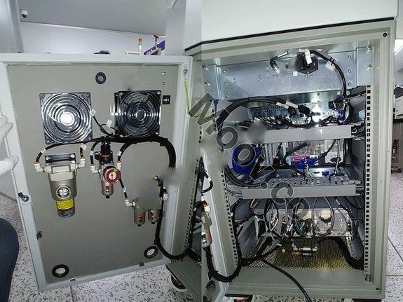
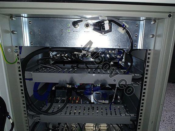
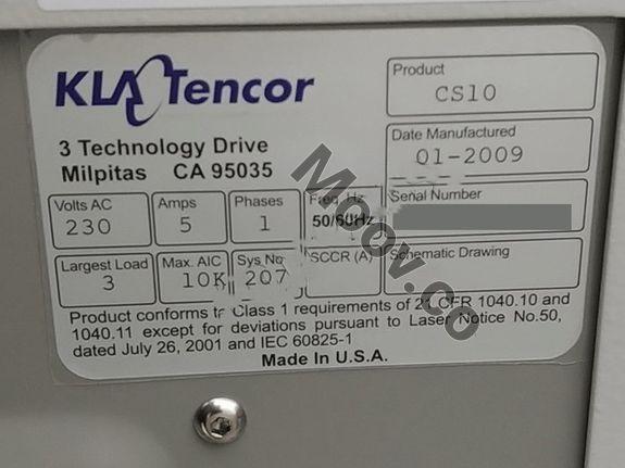
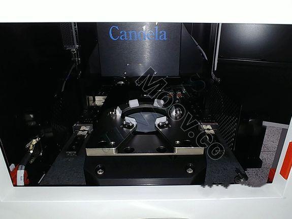
KLA-Tencor Candela CS10V *. Fully refurbished. Installed in Clean-room. Possible demo anytime.Configuration
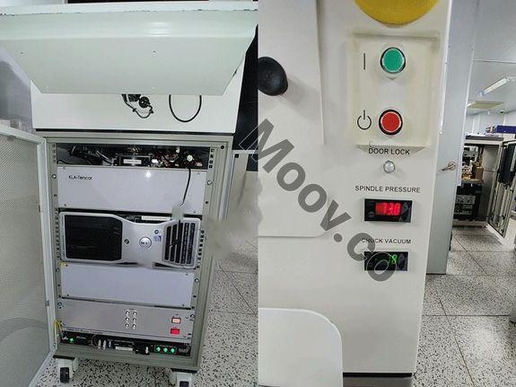
Working Illumination Source : 25 mW laser, 405 nm wavelength Operator Interface : Trackball and keyboard standard Substrate Thickness : 350 μm ~ 1,100 μm Substrate Material : Any clear or opaque polished surface [ Performance ] Defect Sensitivity 0.08 μm diameter PSL sphere equivalent > 95% capture rate(PSL on bare Si) Other Defects and Applications : Particles, scratches, stains, pits, and bumps. Sensitivity: Minimum detectable size for automatic defect classification: - Scratches: 100 μm long, 0.1 μm wide, 50 Å; deep. - Pits: 20 μm diameter, 50 Å; deep - Stains: 20 μm diameter, 10 Å; thick [ Application ] - Opaque substrates - EPI Layers - Transparent film coatings (SiC, GaN, Sapphire)OEM Model Description
The Candela CS10 Optical Surface Analyzer is a compact device that offers exceptional sensitivity to particles and scratches on 2"-12" wafers using dual-laser Optical X-Beam technology. It simultaneously measures phase shift, scattered light, reflected light, and topography to detect and classify wafer surface defects. It is well-suited for laboratory and low volume production applications, and is easy to learn and operate.Documents
No documents

Verified
CATEGORY
Defect Inspection
Last Verified: 5 days ago
Key Item Details
Condition:
Refurbished
Operational Status:
Unknown
Product ID:
65978
Wafer Sizes:
4"/100mm
Vintage:
2009
Logistics Support
Available
Transaction Insured by Moov
Available
Refurbishment Services
Available
Similar Listings
View All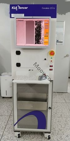


KLA
CANDELA CS10
CATEGORY
Defect Inspection
Last Verified: 5 days ago

Key Item Details
Condition:
Refurbished
Operational Status:
Unknown
Product ID:
65978
Wafer Sizes:
4"/100mm
Vintage:
2009
Logistics Support
Available
Transaction Insured by Moov
Available
Refurbishment Services
Available
Description
KLA-Tencor Candela CS10V *. Fully refurbished. Installed in Clean-room. Possible demo anytime.Configuration
Working Illumination Source : 25 mW laser, 405 nm wavelength Operator Interface : Trackball and keyboard standard Substrate Thickness : 350 μm ~ 1,100 μm Substrate Material : Any clear or opaque polished surface [ Performance ] Defect Sensitivity 0.08 μm diameter PSL sphere equivalent > 95% capture rate(PSL on bare Si) Other Defects and Applications : Particles, scratches, stains, pits, and bumps. Sensitivity: Minimum detectable size for automatic defect classification: - Scratches: 100 μm long, 0.1 μm wide, 50 Å; deep. - Pits: 20 μm diameter, 50 Å; deep - Stains: 20 μm diameter, 10 Å; thick [ Application ] - Opaque substrates - EPI Layers - Transparent film coatings (SiC, GaN, Sapphire)OEM Model Description
The Candela CS10 Optical Surface Analyzer is a compact device that offers exceptional sensitivity to particles and scratches on 2"-12" wafers using dual-laser Optical X-Beam technology. It simultaneously measures phase shift, scattered light, reflected light, and topography to detect and classify wafer surface defects. It is well-suited for laboratory and low volume production applications, and is easy to learn and operate.Documents
No documents