


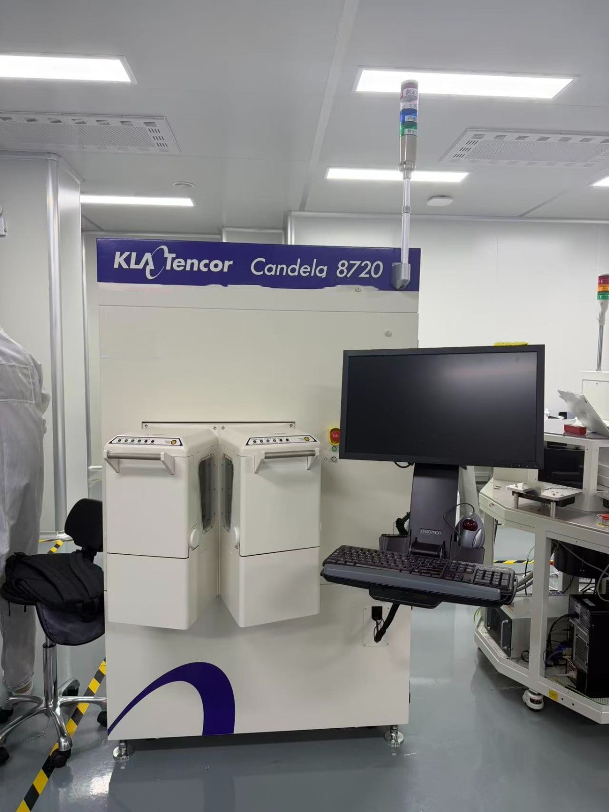
Description
KLA Candela 8720 Surface Defect Inspection System, 2" Optical System Unit Laser Light Source: - 405 nm Laser Diode - 660 nmLaser Diode Detection Channel: - Scatter (Oblique, Normal) - Specular -Topography - Phase - PL (Option) Transfer Unit - Single Wafer Loading: Automatic Transfer by Wafer Transfer Robot - Optical Notch Detection / Flat Detection Mode - Wafer Thickness Detection: Laser Transmission Thickness Detection Module (DTD), Laser Diode 660 nm Computer Unit - CPU: XEON E5-2620 2.0 GHz, 20 MB cache - HDD: 3TB - Network Card: Ether Network Card - Monitor: 19 inch LCD Monitor - Pointing Device: Optical Trackball Software: - Operating System: Microsoft Windows Server 2008 Operating system (English Version) - Candela 8720 Application Software: Version 10 Custom Specifications: - A transformer for stepping up the power supply voltage from 200 V to 230 V - Aligner is brokenConfiguration
No ConfigurationOEM Model Description
The Candela 8720 wafer inspection system uses proprietary optical technology to detect and classify a broad range of defects on high-end compound semiconductor materials up to 200mm in diameter. It is suitable for macro and micro defects and has various use cases in quality control, process control, and vendor comparison. It is used in industries such as HBLED, MicroLED, GaN RF and power applications, and communications. Options include SECS-GEM, light tower, diamond scribe, calibration standards, offline software, OCR, and photoluminescence.Documents
No documents

Verified
CATEGORY
Defect Inspection
Last Verified: Over 30 days ago
Key Item Details
Condition:
Used
Operational Status:
Unknown
Product ID:
150744
Wafer Sizes:
2"/50mm
Vintage:
2018
Logistics Support
Available
Transaction Insured by Moov
Available
Refurbishment Services
Available
Similar Listings
View All


KLA
CANDELA 8720
CATEGORY
Defect Inspection
Last Verified: Over 30 days ago


Key Item Details
Condition:
Used
Operational Status:
Unknown
Product ID:
150744
Wafer Sizes:
2"/50mm
Vintage:
2018
Logistics Support
Available
Transaction Insured by Moov
Available
Refurbishment Services
Available
Description
KLA Candela 8720 Surface Defect Inspection System, 2" Optical System Unit Laser Light Source: - 405 nm Laser Diode - 660 nmLaser Diode Detection Channel: - Scatter (Oblique, Normal) - Specular -Topography - Phase - PL (Option) Transfer Unit - Single Wafer Loading: Automatic Transfer by Wafer Transfer Robot - Optical Notch Detection / Flat Detection Mode - Wafer Thickness Detection: Laser Transmission Thickness Detection Module (DTD), Laser Diode 660 nm Computer Unit - CPU: XEON E5-2620 2.0 GHz, 20 MB cache - HDD: 3TB - Network Card: Ether Network Card - Monitor: 19 inch LCD Monitor - Pointing Device: Optical Trackball Software: - Operating System: Microsoft Windows Server 2008 Operating system (English Version) - Candela 8720 Application Software: Version 10 Custom Specifications: - A transformer for stepping up the power supply voltage from 200 V to 230 V - Aligner is brokenConfiguration
No ConfigurationOEM Model Description
The Candela 8720 wafer inspection system uses proprietary optical technology to detect and classify a broad range of defects on high-end compound semiconductor materials up to 200mm in diameter. It is suitable for macro and micro defects and has various use cases in quality control, process control, and vendor comparison. It is used in industries such as HBLED, MicroLED, GaN RF and power applications, and communications. Options include SECS-GEM, light tower, diamond scribe, calibration standards, offline software, OCR, and photoluminescence.Documents
No documents