




Description
No descriptionConfiguration
- Cassette Handling - Laser: Oblique(50mW, 405nm), Normal(85mW, 660nm) - Spot size: 5㎛ x 4㎛. - Handler: Mapping, Wafer centering on chuck and FFM: OK, Wafer loading/unloading: OK - Particle detection: smaller than 0.08㎛ on silicon substrate. - Scratch: 0.1㎛ wide, 1~2nm deep. - Pits and Bumps: 20㎛ diameter, 50Å; deep. - Stains: 20㎛ diameter, 10Å; thick. - can be used for both epi and bare substrate. - can be used for Si, GaAs, Al2O3,SiC substrate. - Substrate thickness: 350㎛ ~ 1,300㎛. - Air Balance system ULPA and HEPA air filter(replaced new one). - Input Power 115V 12A 50/60Hz - Input Air: CDA 90 PSI - Option: Cognex Wafer IDOEM Model Description
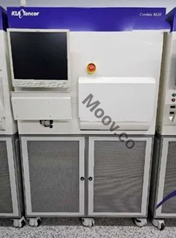
The Candela 8620 is an automated defect inspection system for LED substrates and epitaxy wafers. It provides enhanced quality control for materials such as gallium nitride, sapphire, and silicon carbide. Its proprietary optical design and detection technology can detect sub-micron defects that are not consistently identified by current inspection methods. This enables a production line monitor for yield-limiting defects, improving MOCVD reactor uptime and yield. The system can detect defects such as micro-scratches, micro-cracks, missing bumps, resist voids, hexagonal pits, and epi cracks, which can impact device performance, yield, and reliability.Documents
No documents

Verified
CATEGORY
Defect Inspection
Last Verified: 9 days ago
Key Item Details
Condition:
Refurbished
Operational Status:
Unknown
Product ID:
153576
Wafer Sizes:
8"/200mm
Vintage:
Unknown
Logistics Support
Available
Transaction Insured by Moov
Available
Refurbishment Services
Available
Similar Listings
View All



KLA
CANDELA 8620
CATEGORY
Defect Inspection
Last Verified: 9 days ago


Key Item Details
Condition:
Refurbished
Operational Status:
Unknown
Product ID:
153576
Wafer Sizes:
8"/200mm
Vintage:
Unknown
Logistics Support
Available
Transaction Insured by Moov
Available
Refurbishment Services
Available
Description
No descriptionConfiguration
- Cassette Handling - Laser: Oblique(50mW, 405nm), Normal(85mW, 660nm) - Spot size: 5㎛ x 4㎛. - Handler: Mapping, Wafer centering on chuck and FFM: OK, Wafer loading/unloading: OK - Particle detection: smaller than 0.08㎛ on silicon substrate. - Scratch: 0.1㎛ wide, 1~2nm deep. - Pits and Bumps: 20㎛ diameter, 50Å; deep. - Stains: 20㎛ diameter, 10Å; thick. - can be used for both epi and bare substrate. - can be used for Si, GaAs, Al2O3,SiC substrate. - Substrate thickness: 350㎛ ~ 1,300㎛. - Air Balance system ULPA and HEPA air filter(replaced new one). - Input Power 115V 12A 50/60Hz - Input Air: CDA 90 PSI - Option: Cognex Wafer IDOEM Model Description
The Candela 8620 is an automated defect inspection system for LED substrates and epitaxy wafers. It provides enhanced quality control for materials such as gallium nitride, sapphire, and silicon carbide. Its proprietary optical design and detection technology can detect sub-micron defects that are not consistently identified by current inspection methods. This enables a production line monitor for yield-limiting defects, improving MOCVD reactor uptime and yield. The system can detect defects such as micro-scratches, micro-cracks, missing bumps, resist voids, hexagonal pits, and epi cracks, which can impact device performance, yield, and reliability.Documents
No documents