


Description
No descriptionConfiguration
details attached.OEM Model Description
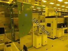
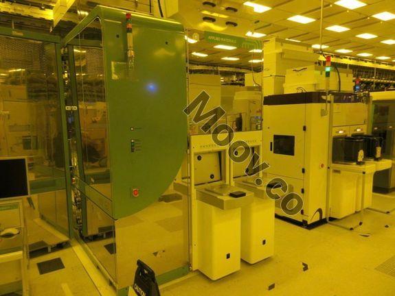
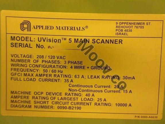
The Applied UVision 5 wafer inspection system detects yield-limiting defects in the critical patterning layers of 22nm and below logic and memory devices. Applied also offers the Applied DFinder system, the first darkfield wafer inspection system to use DUV laser scanning to detect particles as small as 40nm in interconnect layers. The UVision® 5 system isa member of the UVision wafer inspection product family, supporting the same proprietary core technology of deep ultraviolet (DUV) laser illumination, with simultaneous dual channel [brightfield (BF) reflected light and grayfield (GF) scattered light] collection optics. The system exhibits new defect inspection capabilities on advanced patterning layers in both FEOL and BEOL applications for 2xnm production and beyond, addressing such technologies as ArF immersion lithography, double and quad patterning, and extreme ultraviolet layers. The UVision 5 system’s dramatically increased light density enables detection of 1xnm killer defects - some never captured before - resulting in a twofold improvement in killer defect capture rates. This, in turn, results in a more accurate and comprehensive defect Pareto that significantly improves statistical process control in the wafer fab. The platform’s unique GF detection architecture now captures more light to enable detection of defects in the range of 1xnm (approximately the width of up to five DNA strands). New imaging modes improve detection sensitivity to further increase UVision technology leadership in GF scanning. Novel image processing algorithms reduce wafer noise by up to 50% in various types of memory structures, contributing to a higher capture rate, especially on BEOL layers.Documents

CATEGORY
Defect Inspection
Last Verified: Over 60 days ago
Key Item Details
Condition:
Used
Operational Status:
Unknown
Product ID:
68079
Wafer Sizes:
12"/300mm
Vintage:
2011
Logistics Support
Available
Transaction Insured by Moov
Available
Refurbishment Services
Available
Similar Listings
View All
APPLIED MATERIALS (AMAT)
UVISION 5
CATEGORY
Defect Inspection
Last Verified: Over 60 days ago

Key Item Details
Condition:
Used
Operational Status:
Unknown
Product ID:
68079
Wafer Sizes:
12"/300mm
Vintage:
2011
Logistics Support
Available
Transaction Insured by Moov
Available
Refurbishment Services
Available