


Description
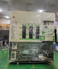
Nikon KrF lithography machines use 248nm wavelength KrF excimer lasers as exposure light sources, which are suitable for more sophisticated semiconductor processes and are widely used in the manufacture of high-performance semiconductor devices, including microprocessors, dynamic random access memory (DRAM), and complex logic and mixed signal chips. These lithography machines are key equipment for achieving high-precision semiconductor device manufacturing, and play an important role in 4-inch, 6-inch, 8-inch and 12-inch wafer production lines, providing semiconductor manufacturers with flexibility and efficient production capabilities.Configuration
0.20 0.68 4:1 25*33 LSA:40 FIA:45OEM Model Description
The system offers a resolution of 150 nm or better with a numerical aperture (NA) of 0.68. It utilizes a KrF excimer laser with a wavelength of 248 nm as the exposure light source. The reduction ratio is 1:4, and the exposure field measures 25 × 33 mm. The alignment accuracy, using the EGA method with |M| + 3σ, is equal to or less than 35 nm.Documents
No documents

Key Item Details
Condition:
Used
Operational Status:
Unknown
Product ID:
131672
Wafer Sizes:
4"/100mm, 6"/150mm, 8"/200mm, 12"/300mm
Vintage:
Unknown
Logistics Support
Available
Transaction Insured by Moov
Available
Refurbishment Services
Available
Similar Listings
View All


NIKON
NSR-S204B
CATEGORY
Steppers & Scanners
Last Verified: Over 60 days ago


Key Item Details
Condition:
Used
Operational Status:
Unknown
Product ID:
131672
Wafer Sizes:
4"/100mm, 6"/150mm, 8"/200mm, 12"/300mm
Vintage:
Unknown
Logistics Support
Available
Transaction Insured by Moov
Available
Refurbishment Services
Available
Description
Nikon KrF lithography machines use 248nm wavelength KrF excimer lasers as exposure light sources, which are suitable for more sophisticated semiconductor processes and are widely used in the manufacture of high-performance semiconductor devices, including microprocessors, dynamic random access memory (DRAM), and complex logic and mixed signal chips. These lithography machines are key equipment for achieving high-precision semiconductor device manufacturing, and play an important role in 4-inch, 6-inch, 8-inch and 12-inch wafer production lines, providing semiconductor manufacturers with flexibility and efficient production capabilities.Configuration
0.20 0.68 4:1 25*33 LSA:40 FIA:45OEM Model Description
The system offers a resolution of 150 nm or better with a numerical aperture (NA) of 0.68. It utilizes a KrF excimer laser with a wavelength of 248 nm as the exposure light source. The reduction ratio is 1:4, and the exposure field measures 25 × 33 mm. The alignment accuracy, using the EGA method with |M| + 3σ, is equal to or less than 35 nm.Documents
No documents