
Description
No descriptionConfiguration
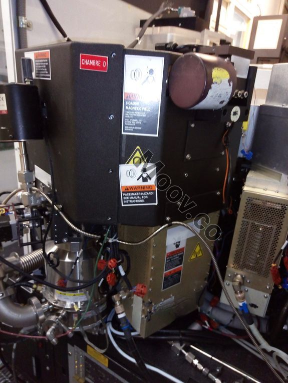
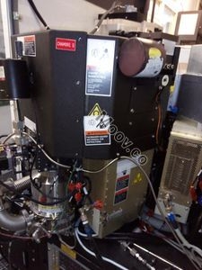
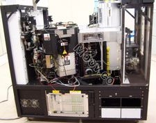
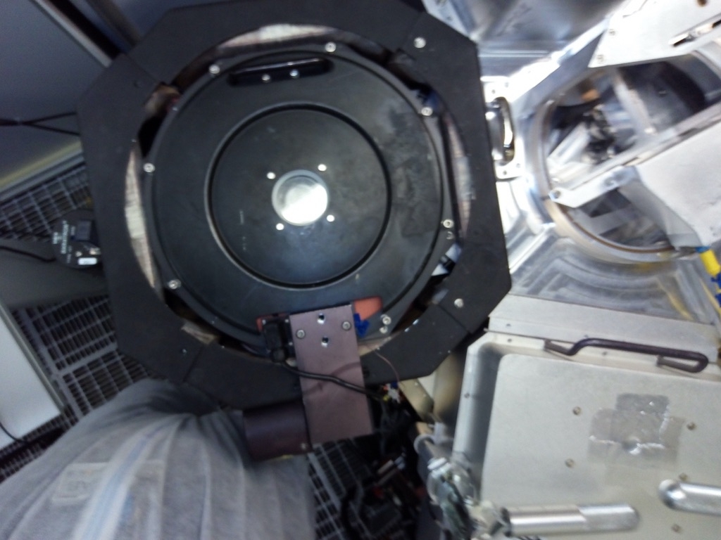
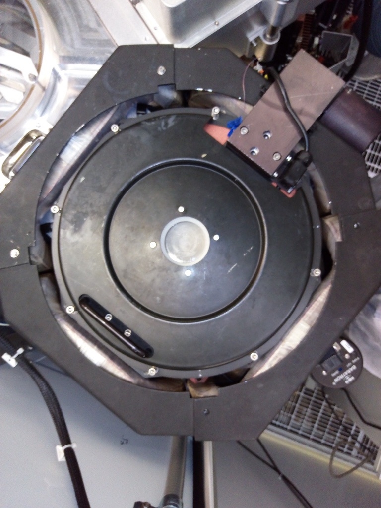
Mark II Sput Etch Chamber (chamber only) Process Kits: – 0020-10518 Pedestal – 3690-01364 Graphite Ring – 0200-09086 Pedestal QTZ Ring – 0020-09933 GDP Anodized Aluminum Turbo : Seiko-Seiki Edwards STP301CVB Match Box: 0010-09416OEM Model Description
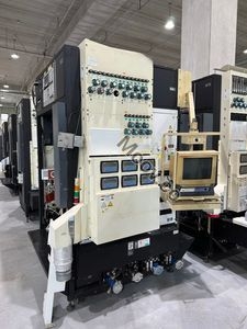
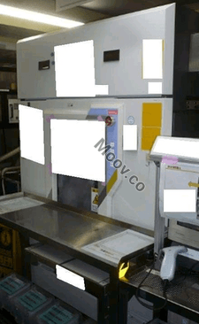
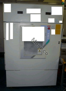
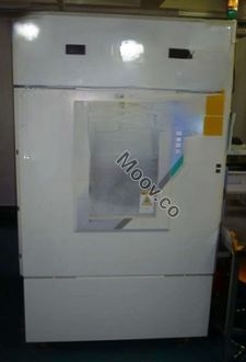
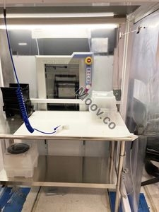
The AMAT P5000 Etch is a magnetically enhanced reactive ion etching system (MERIE) with two functional process chambers (Chambers B & C). P5000 Chamber B is primarily used for etching silicon based dielectrics (silicon dioxide, silcon nitride, etc.) and some carbon based compounds (resist, poly imide, etc) while chamber C is mainly used for silicon etching with high selectivity to underlying dielectric such as silicon dioxide. The system can process only 4" wafers. Pieces have to be attached to a 4" wafer. Though the process chamber processes one wafer at a time, up to 25 wafers can be loaded per batch.Documents
No documents
APPLIED MATERIALS (AMAT)
P5000 ETCH

Verified
CATEGORY
RIE
Last Verified: Over 30 days ago
Key Item Details
Condition:
Used
Operational Status:
Unknown
Product ID:
68081
Wafer Sizes:
Unknown
Vintage:
Unknown
Have Additional Questions?
Logistics Support
Available
Money Back Guarantee
Available
Transaction Insured by Moov
Available
Refurbishment Services
Available
Similar Listings
View All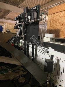


APPLIED MATERIALS (AMAT)
P5000 ETCH
CATEGORY
RIE
Last Verified: Over 30 days ago


Key Item Details
Condition:
Used
Operational Status:
Unknown
Product ID:
68081
Wafer Sizes:
Unknown
Vintage:
Unknown
Logistics Support
Available
Money Back Guarantee
Available
Transaction Insured by Moov
Available
Refurbishment Services
Available
Description
No descriptionConfiguration
Mark II Sput Etch Chamber (chamber only) Process Kits: – 0020-10518 Pedestal – 3690-01364 Graphite Ring – 0200-09086 Pedestal QTZ Ring – 0020-09933 GDP Anodized Aluminum Turbo : Seiko-Seiki Edwards STP301CVB Match Box: 0010-09416OEM Model Description
The AMAT P5000 Etch is a magnetically enhanced reactive ion etching system (MERIE) with two functional process chambers (Chambers B & C). P5000 Chamber B is primarily used for etching silicon based dielectrics (silicon dioxide, silcon nitride, etc.) and some carbon based compounds (resist, poly imide, etc) while chamber C is mainly used for silicon etching with high selectivity to underlying dielectric such as silicon dioxide. The system can process only 4" wafers. Pieces have to be attached to a 4" wafer. Though the process chamber processes one wafer at a time, up to 25 wafers can be loaded per batch.Documents
No documents