


Description
No descriptionConfiguration
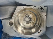
3 DxZ Chambers w/ RPSOEM Model Description
The Centura 5200 DXZ is used for advanced 150mm and 200mm CVD technology in the advanced CMOS and MtM segments. It can be used for ultra-thick oxides (≥20µm), low-temperature processing (<200°C), conformal, low wet-etch-rate films, and doped films with tunable refractive indices. The system can handle a variety of MtM substrates (including SiC wafers) reliably and carefully from load lock wafer mapping to clear wafer orientation to wafer placement.Documents
No documents

CATEGORY
PECVD
Last Verified: Over 60 days ago
Key Item Details
Condition:
Used
Operational Status:
Unknown
Product ID:
15128
Wafer Sizes:
8"/200mm
Vintage:
Unknown
Logistics Support
Available
Transaction Insured by Moov
Available
Refurbishment Services
Available

APPLIED MATERIALS (AMAT)
CENTURA 5200 DXZ
CATEGORY
PECVD
Last Verified: Over 60 days ago


Key Item Details
Condition:
Used
Operational Status:
Unknown
Product ID:
15128
Wafer Sizes:
8"/200mm
Vintage:
Unknown
Logistics Support
Available
Transaction Insured by Moov
Available
Refurbishment Services
Available
Description
No descriptionConfiguration
3 DxZ Chambers w/ RPSOEM Model Description
The Centura 5200 DXZ is used for advanced 150mm and 200mm CVD technology in the advanced CMOS and MtM segments. It can be used for ultra-thick oxides (≥20µm), low-temperature processing (<200°C), conformal, low wet-etch-rate films, and doped films with tunable refractive indices. The system can handle a variety of MtM substrates (including SiC wafers) reliably and carefully from load lock wafer mapping to clear wafer orientation to wafer placement.Documents
No documents