


Description
No descriptionConfiguration
Automated Mask Aligner Wafer Size: 8" Equipment Configuration: Wafer Configuration: 9" inch mask holder square, 8" wafer chuckDouble-sided/Backside Alignment Capability Manual Load Motorized illuminator 1000w lamp (joystick)- Manual XYZ stage (coarse and finePCadiustments-Includes:Lamp,MirrorandOptOEM Model Description
The EVG6200∞ Alignment System is a high-throughput, reliable, and accurate system for handling wafers and substrates up to 200mm. It features EV Group’s NanoAlign Technology for high alignment accuracy and resolution, making it competitive in full-field lithography. It is designed for wafer bumping, chip scale packaging, MEMS, Compound Semiconductor, Power Devices, and Nanotechnology applications. The system has a high degree of automation and can handle multiple wafer sizes with quick change-over time. It also has options for cassette-to-cassette handling, automatic alignment, and field upgrades.Documents
No documents

Verified
CATEGORY
Mask/Bond Aligners
Last Verified: Over 60 days ago
Key Item Details
Condition:
Used
Operational Status:
Unknown
Product ID:
120507
Wafer Sizes:
8"/200mm
Vintage:
2004
Logistics Support
Available
Transaction Insured by Moov
Available
Refurbishment Services
Available
Similar Listings
View All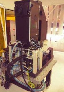


EVGroup (EVG)
EVG6200-Infinity
CATEGORY
Mask/Bond Aligners
Last Verified: Over 60 days ago


Key Item Details
Condition:
Used
Operational Status:
Unknown
Product ID:
120507
Wafer Sizes:
8"/200mm
Vintage:
2004
Logistics Support
Available
Transaction Insured by Moov
Available
Refurbishment Services
Available
Description
No descriptionConfiguration
Automated Mask Aligner Wafer Size: 8" Equipment Configuration: Wafer Configuration: 9" inch mask holder square, 8" wafer chuckDouble-sided/Backside Alignment Capability Manual Load Motorized illuminator 1000w lamp (joystick)- Manual XYZ stage (coarse and finePCadiustments-Includes:Lamp,MirrorandOptOEM Model Description
The EVG6200∞ Alignment System is a high-throughput, reliable, and accurate system for handling wafers and substrates up to 200mm. It features EV Group’s NanoAlign Technology for high alignment accuracy and resolution, making it competitive in full-field lithography. It is designed for wafer bumping, chip scale packaging, MEMS, Compound Semiconductor, Power Devices, and Nanotechnology applications. The system has a high degree of automation and can handle multiple wafer sizes with quick change-over time. It also has options for cassette-to-cassette handling, automatic alignment, and field upgrades.Documents
No documents