


Description
No descriptionConfiguration
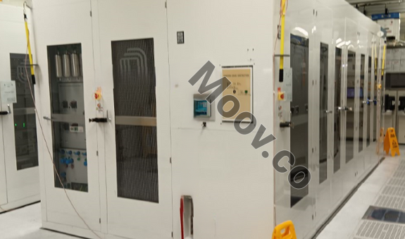
IBA_HiCurOEM Model Description
The Applied Quantum X Implant system, along with Applied's other technologies, meets the strict requirements for 65nm transistors. It offers high throughput at low energies, uniformity across all points and wafers, and precise motion control to prevent particle damage. The system is extendible to new applications for advanced logic and memory devices. Quantum X redefines fab productivity for high current ion implantation by providing single-wafer precision, ultra-low defect levels, and high throughput. Its innovative technology enables extendibility to high tilt implant and other new applications at 65nm and beyond. It features high throughput at low energies (200eV - 80keV) with all points, all wafers uniformity and two-dimensional parallel scanning with StepScan™ fixed beam technology for single wafer processing and up to 60° tilt angleDocuments
No documents

CATEGORY
High Current
Last Verified: 22 days ago
Key Item Details
Condition:
Used
Operational Status:
Unknown
Product ID:
144803
Wafer Sizes:
12"/300mm
Vintage:
2006
Logistics Support
Available
Transaction Insured by Moov
Available
Refurbishment Services
Available
Similar Listings
View All


APPLIED MATERIALS (AMAT)
QUANTUM X
CATEGORY
High Current
Last Verified: 22 days ago


Key Item Details
Condition:
Used
Operational Status:
Unknown
Product ID:
144803
Wafer Sizes:
12"/300mm
Vintage:
2006
Logistics Support
Available
Transaction Insured by Moov
Available
Refurbishment Services
Available
Description
No descriptionConfiguration
IBA_HiCurOEM Model Description
The Applied Quantum X Implant system, along with Applied's other technologies, meets the strict requirements for 65nm transistors. It offers high throughput at low energies, uniformity across all points and wafers, and precise motion control to prevent particle damage. The system is extendible to new applications for advanced logic and memory devices. Quantum X redefines fab productivity for high current ion implantation by providing single-wafer precision, ultra-low defect levels, and high throughput. Its innovative technology enables extendibility to high tilt implant and other new applications at 65nm and beyond. It features high throughput at low energies (200eV - 80keV) with all points, all wafers uniformity and two-dimensional parallel scanning with StepScan™ fixed beam technology for single wafer processing and up to 60° tilt angleDocuments
No documents