



Description
CVDConfiguration
No ConfigurationOEM Model Description
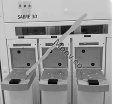
The SABRE 3D electroplating system is a highly flexible and modular architecture that can perform a wide range of high-productivity wafer-level packaging (WLP) processes. These include copper through-silicon vias (TSV), copper redistribution layers (RDL), pillars, under-bump metallization, and lead-free micro-bumping. It is specifically designed for the advanced WLP market. The Sabre 3D can produce wafers up to 12 inches in size and has a TSV ECP of 12 inches . The system incorporates many of the technologies used in the SABRE platform, such as sealed dry contacts, innovative clamshell and cell design, SmartDose bath control, and precision wafer handling.Documents
No documents

Verified
CATEGORY
Electro Plating
Last Verified: Over 60 days ago
Key Item Details
Condition:
Used
Operational Status:
Unknown
Product ID:
149442
Wafer Sizes:
12"/300mm
Vintage:
Unknown
Logistics Support
Available
Transaction Insured by Moov
Available
Refurbishment Services
Available
Similar Listings
View All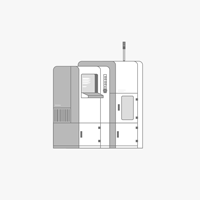
LAM RESEARCH / NOVELLUS
SABRE 3D
CATEGORY
Electro Plating
Last Verified: Over 60 days ago


Key Item Details
Condition:
Used
Operational Status:
Unknown
Product ID:
149442
Wafer Sizes:
12"/300mm
Vintage:
Unknown
Logistics Support
Available
Transaction Insured by Moov
Available
Refurbishment Services
Available
Description
CVDConfiguration
No ConfigurationOEM Model Description
The SABRE 3D electroplating system is a highly flexible and modular architecture that can perform a wide range of high-productivity wafer-level packaging (WLP) processes. These include copper through-silicon vias (TSV), copper redistribution layers (RDL), pillars, under-bump metallization, and lead-free micro-bumping. It is specifically designed for the advanced WLP market. The Sabre 3D can produce wafers up to 12 inches in size and has a TSV ECP of 12 inches . The system incorporates many of the technologies used in the SABRE platform, such as sealed dry contacts, innovative clamshell and cell design, SmartDose bath control, and precision wafer handling.Documents
No documents