





Description
- Main Components o Integrated Console o Bare Wafer Inspection Station o Equipment Front End Module (EFEM) o 3-Port Wafer Loading UnitConfiguration
- Inspection Platform o Un-patterned wafer inspection platform with deep-ultraviolet (DUV) illumination o DUV-specific apertures for defect capture on un-patterned thin films o High-speed stage and advanced imaging computer for enhanced productivity o Full-wafer, high-resolution haze maps to generate complete wafer haze maps at high resolution - Defect Capture & Analysis o Engineered to detect a wide spectrum of defect types at 32 nm and 22 nm technology nodes o Automated classification system for rapid, high-volume defect sorting o Precise coordinate mapping for quick re-inspection and review o SURFmonitor haze mapping (~100 megapixel resolution) for: o Identifying micro-scratches and slip lines o Mapping surface roughness, grain size, and other process metrics o Enhanced sensitivity and throughput compared to the Surfscan SP2XP predecessor o Dedicated backside inspection module to identify defects that could distort wafer geometryOEM Model Description
The Surfscan® SP3 is an unpatterned wafer inspection tool available in 450mm, 300mm, and 300mm/450mm bridge tool configurations. It uses deep ultra-violet (DUV) sensitivity and has a throughput up to three times that of its predecessor. It can detect critical defects and surface quality issues for IC, OEM, and substrate manufacturing at the 2Xnm design node. The tool also includes an integrated SURFmonitor module that characterizes and measures surface quality. It has flexible configurations and a reliable, extendible architecture. It is used for qualification and monitoring of process tools for the 2Xnm design node within the IC fab, as well as serving as a lithography process tool monitor. The Surfscan SP3 can also be used for incoming wafer qualification, inline process control, final wafer qualification, process tool qualification, and as a process uniformity monitor.Documents
No documents

Verified
CATEGORY
Defect Inspection
Last Verified: 11 days ago
Key Item Details
Condition:
Used
Operational Status:
Unknown
Product ID:
153388
Wafer Sizes:
12"/300mm
Vintage:
Unknown
Logistics Support
Available
Transaction Insured by Moov
Available
Refurbishment Services
Available
Similar Listings
View All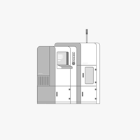
KLA
SURFSCAN SP3
CATEGORY
Defect Inspection
Last Verified: 11 days ago


Key Item Details
Condition:
Used
Operational Status:
Unknown
Product ID:
153388
Wafer Sizes:
12"/300mm
Vintage:
Unknown
Logistics Support
Available
Transaction Insured by Moov
Available
Refurbishment Services
Available
Description
- Main Components o Integrated Console o Bare Wafer Inspection Station o Equipment Front End Module (EFEM) o 3-Port Wafer Loading UnitConfiguration
- Inspection Platform o Un-patterned wafer inspection platform with deep-ultraviolet (DUV) illumination o DUV-specific apertures for defect capture on un-patterned thin films o High-speed stage and advanced imaging computer for enhanced productivity o Full-wafer, high-resolution haze maps to generate complete wafer haze maps at high resolution - Defect Capture & Analysis o Engineered to detect a wide spectrum of defect types at 32 nm and 22 nm technology nodes o Automated classification system for rapid, high-volume defect sorting o Precise coordinate mapping for quick re-inspection and review o SURFmonitor haze mapping (~100 megapixel resolution) for: o Identifying micro-scratches and slip lines o Mapping surface roughness, grain size, and other process metrics o Enhanced sensitivity and throughput compared to the Surfscan SP2XP predecessor o Dedicated backside inspection module to identify defects that could distort wafer geometryOEM Model Description
The Surfscan® SP3 is an unpatterned wafer inspection tool available in 450mm, 300mm, and 300mm/450mm bridge tool configurations. It uses deep ultra-violet (DUV) sensitivity and has a throughput up to three times that of its predecessor. It can detect critical defects and surface quality issues for IC, OEM, and substrate manufacturing at the 2Xnm design node. The tool also includes an integrated SURFmonitor module that characterizes and measures surface quality. It has flexible configurations and a reliable, extendible architecture. It is used for qualification and monitoring of process tools for the 2Xnm design node within the IC fab, as well as serving as a lithography process tool monitor. The Surfscan SP3 can also be used for incoming wafer qualification, inline process control, final wafer qualification, process tool qualification, and as a process uniformity monitor.Documents
No documents