



Description
DarkfieldConfiguration
FrameOEM Model Description
The ComPlus-EV system solution delivers exceptional advantages in system sensitivity and throughput, as well as significant savings to customers who typically purchase multiple highly-specialized inspection tools to cover the same range of applications. Using proprietary EnlargedGrayField technology, the ComPlus-EV detects a broad range of defect types at production speeds, including the most challenging ultra-small and flat pattern defects, as well as CMP(chemical mechanical polishing) copper interconnect and photolithography process defects.The new EZSet automatic recipe creator greatly reduces recipe creation and optimization time, for higher system availability. With its embedded connectivity to the SEMVision(TM) defect review system, ComPlus-EV delivers fast time-to-data for rapid fault detection. The ComPlus-EV can be further enhanced with the MP (Multi-Perspective) option, whichextends the system's exceptional capabilities to perform additional brightfield applications,including the detection of defects in the transistor area such as STI, gate, and tungsten plug layers. The MP option expands the number of detectors and magnifications, enabling higher sensitivity to flat defects at an increased capture rate, providing significantly higher throughput and reduced cost of ownership.Documents
No documents

CATEGORY
Defect Inspection
Last Verified: 18 days ago
Key Item Details
Condition:
Used
Operational Status:
Unknown
Product ID:
155233
Wafer Sizes:
8"/200mm
Vintage:
2003
Logistics Support
Available
Transaction Insured by Moov
Available
Refurbishment Services
Available
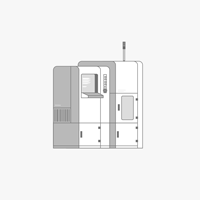
APPLIED MATERIALS (AMAT)
COMPLUS EV
CATEGORY
Defect Inspection
Last Verified: 18 days ago


Key Item Details
Condition:
Used
Operational Status:
Unknown
Product ID:
155233
Wafer Sizes:
8"/200mm
Vintage:
2003
Logistics Support
Available
Transaction Insured by Moov
Available
Refurbishment Services
Available
Description
DarkfieldConfiguration
FrameOEM Model Description
The ComPlus-EV system solution delivers exceptional advantages in system sensitivity and throughput, as well as significant savings to customers who typically purchase multiple highly-specialized inspection tools to cover the same range of applications. Using proprietary EnlargedGrayField technology, the ComPlus-EV detects a broad range of defect types at production speeds, including the most challenging ultra-small and flat pattern defects, as well as CMP(chemical mechanical polishing) copper interconnect and photolithography process defects.The new EZSet automatic recipe creator greatly reduces recipe creation and optimization time, for higher system availability. With its embedded connectivity to the SEMVision(TM) defect review system, ComPlus-EV delivers fast time-to-data for rapid fault detection. The ComPlus-EV can be further enhanced with the MP (Multi-Perspective) option, whichextends the system's exceptional capabilities to perform additional brightfield applications,including the detection of defects in the transistor area such as STI, gate, and tungsten plug layers. The MP option expands the number of detectors and magnifications, enabling higher sensitivity to flat defects at an increased capture rate, providing significantly higher throughput and reduced cost of ownership.Documents
No documents