



Description
No descriptionConfiguration
No ConfigurationOEM Model Description
The Applied SEMVision G7 system offers greater imaging variety and advances in automatic defect classification (ADC) based on expanded machine learning capabilities. Besides the imaging capabilities of the previous SEMVision generation, the new system offers unique imaging of the wafer-edge bevel and apex where undetected defects can reduce device yield. To achieve robust review of unpatterned wafers, an enhanced light source and collection mechanism combined with improved noise suppression enable optical detection of defects as small as 18nm.Documents
No documents

CATEGORY
Defect Inspection
Last Verified: Over 60 days ago
Key Item Details
Condition:
Used
Operational Status:
Unknown
Product ID:
150294
Wafer Sizes:
Unknown
Vintage:
Unknown
Logistics Support
Available
Transaction Insured by Moov
Available
Refurbishment Services
Available
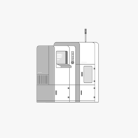
APPLIED MATERIALS (AMAT)
SEMVISION G7
CATEGORY
Defect Inspection
Last Verified: Over 60 days ago


Key Item Details
Condition:
Used
Operational Status:
Unknown
Product ID:
150294
Wafer Sizes:
Unknown
Vintage:
Unknown
Logistics Support
Available
Transaction Insured by Moov
Available
Refurbishment Services
Available
Description
No descriptionConfiguration
No ConfigurationOEM Model Description
The Applied SEMVision G7 system offers greater imaging variety and advances in automatic defect classification (ADC) based on expanded machine learning capabilities. Besides the imaging capabilities of the previous SEMVision generation, the new system offers unique imaging of the wafer-edge bevel and apex where undetected defects can reduce device yield. To achieve robust review of unpatterned wafers, an enhanced light source and collection mechanism combined with improved noise suppression enable optical detection of defects as small as 18nm.Documents
No documents