



Description
No descriptionConfiguration
Bow Warp +- .5um Thickness Repeatability 35nm+ _200/300mm 4 station sorter with Al subframe and locator plates _white powder coated lockable system panels _sub-class 1 integrated mini environment _900mm load height _industry standard Sankyo robotics SR8241 dual yaw trackless robot _dual vacuum backside EEF's to accommodate 300mm wafers _industry standard Logosol three axis vacuum backside pre-aligner _industry standard Sinfonia 300mm FOUP/FOSB loadports - qty 2 _enclosed open cassette stages with locator blocks - qty 2 _single industry standard IOSS WID120 OCR reader for TOPSIDE scribes _RFID and E84 kits per tool - qty 2 _integrated ionization system - ION bar + controller _includes infrastructure for extra bottomside camera _backup vacuum reservoir for fail over operation _backup 220V UPS for fail over operation _IPC I7 class system computer operating at 3.2Ghz with 16G RAM & >1TB HD _additional 4TB HD for inspection results _Microsoft Windows 10 64bit LTSC operating system (EOL 2032) _NADAtech NS300 software with RBuilder recipe development tool _RBuilder extensions for customer specific JobFile based sorting _RBuilder extensions for wafer sleuth compatibility _RBuilder extensions for auto carrier type detect _RBuilder extensions for, +THK, +BWT, +MIDS, +ChipChecker _NADAtech factory USB system backup _SEMI E4-0307 (SECS-I) _SEMI E5-0220 (SECS-II) _SEMI E30-0520 (GEM) _SEMI E37-0819 (HSMS) _SEMI E39-0703 (Obj Services) _SEMI E40-1218 (Processing) _SEMI E58-0703 (ARAMS) _SEMI E84-1109 (OHT handoff) _SEMI E87-0619 (CMS) _SEMI E90-0312 (Substrate Tracking) _SEMI E94-0314 (Control Job) multi-point thickness measurement at customer specified points around wafer via dual chromatic confocal dual point sensors differential white light sensors + ultra low CTE mounting hardware _wafer thickness range from 300um to 1500um _automatic gauge block for measurement calibration _programmable measurement points _wafer thickness map _CSV results file *35nm repeatability *no temperature correction inspection cell for high throughput bow / warp / thickness measurements via stationary non-contact OCT scanning sensor _BOLTS compliant module for attachment to t series platform _vibration isolation inside modular enclosure ensuring stable and precise measurements _class 1 FFU for clean environment _3 pin mounting/leveling stage for precise wafer placement with sensor assembly for wafer detection _310mm FOV Flying Spot Sensor for bow / warp / thickness measurements _standard recipe setup for 200 and 300mm _GUI setup utility for standard or custom scanning patterns _standard output analysis for BW, AvgTHK, TTV, LTV, SQFR _result images local or shared network in .png file format _3D visualization tool _CSV measurement file output to local or shared network _per wafer GEM/SECS CEID events for all +BWT data with OCR _final wafer map report with +BWT values _GEM300 extensions for JobFile based inspections *±.5μm repeatabilityOEM Model Description
None ProvidedDocuments
No documents

NADAtech
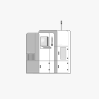
T4A4
CATEGORY
Wafer Handling
Last Verified: Over 30 days ago


Key Item Details
Condition:
Used
Operational Status:
Unknown
Product ID:
150754
Wafer Sizes:
8"/200mm, 12"/300mm
Vintage:
Unknown
Logistics Support
Available
Transaction Insured by Moov
Available
Refurbishment Services
Available
Description
No descriptionConfiguration
Bow Warp +- .5um Thickness Repeatability 35nm+ _200/300mm 4 station sorter with Al subframe and locator plates _white powder coated lockable system panels _sub-class 1 integrated mini environment _900mm load height _industry standard Sankyo robotics SR8241 dual yaw trackless robot _dual vacuum backside EEF's to accommodate 300mm wafers _industry standard Logosol three axis vacuum backside pre-aligner _industry standard Sinfonia 300mm FOUP/FOSB loadports - qty 2 _enclosed open cassette stages with locator blocks - qty 2 _single industry standard IOSS WID120 OCR reader for TOPSIDE scribes _RFID and E84 kits per tool - qty 2 _integrated ionization system - ION bar + controller _includes infrastructure for extra bottomside camera _backup vacuum reservoir for fail over operation _backup 220V UPS for fail over operation _IPC I7 class system computer operating at 3.2Ghz with 16G RAM & >1TB HD _additional 4TB HD for inspection results _Microsoft Windows 10 64bit LTSC operating system (EOL 2032) _NADAtech NS300 software with RBuilder recipe development tool _RBuilder extensions for customer specific JobFile based sorting _RBuilder extensions for wafer sleuth compatibility _RBuilder extensions for auto carrier type detect _RBuilder extensions for, +THK, +BWT, +MIDS, +ChipChecker _NADAtech factory USB system backup _SEMI E4-0307 (SECS-I) _SEMI E5-0220 (SECS-II) _SEMI E30-0520 (GEM) _SEMI E37-0819 (HSMS) _SEMI E39-0703 (Obj Services) _SEMI E40-1218 (Processing) _SEMI E58-0703 (ARAMS) _SEMI E84-1109 (OHT handoff) _SEMI E87-0619 (CMS) _SEMI E90-0312 (Substrate Tracking) _SEMI E94-0314 (Control Job) multi-point thickness measurement at customer specified points around wafer via dual chromatic confocal dual point sensors differential white light sensors + ultra low CTE mounting hardware _wafer thickness range from 300um to 1500um _automatic gauge block for measurement calibration _programmable measurement points _wafer thickness map _CSV results file *35nm repeatability *no temperature correction inspection cell for high throughput bow / warp / thickness measurements via stationary non-contact OCT scanning sensor _BOLTS compliant module for attachment to t series platform _vibration isolation inside modular enclosure ensuring stable and precise measurements _class 1 FFU for clean environment _3 pin mounting/leveling stage for precise wafer placement with sensor assembly for wafer detection _310mm FOV Flying Spot Sensor for bow / warp / thickness measurements _standard recipe setup for 200 and 300mm _GUI setup utility for standard or custom scanning patterns _standard output analysis for BW, AvgTHK, TTV, LTV, SQFR _result images local or shared network in .png file format _3D visualization tool _CSV measurement file output to local or shared network _per wafer GEM/SECS CEID events for all +BWT data with OCR _final wafer map report with +BWT values _GEM300 extensions for JobFile based inspections *±.5μm repeatabilityOEM Model Description
None ProvidedDocuments
No documents