


Description
Nikon KrF lithography machines use 248nm wavelength KrF excimer lasers as exposure light sources, which are suitable for more sophisticated semiconductor processes and are widely used in the manufacture of high-performance semiconductor devices, including microprocessors, dynamic random access memory (DRAM), and complex logic and mixed signal chips. These lithography machines are key equipment for achieving high-precision semiconductor device manufacturing, and play an important role in 4-inch, 6-inch, 8-inch and 12-inch wafer production lines, providing semiconductor manufacturers with flexibility and efficient production capabilities.Configuration
Scanning LSA:35 0.15 0.75 4:1 25*33 FIA:40OEM Model Description
This Nikon Step-and-Repeat Scanning System is compatible with both 200mm and 300mm process nodes and has a resolution of resolution ≦ 130 nm. When the NSR S205C was originally released in 2000, it boasted the the world's first ultra-high N.A. (0.75) projection lens as well as a KrF excimer laser. The system can process 140+ 200mm wafers/hour (16% higher throughput than Nikon's previous system). Applications for the NSR S205C include mass production of DRAM and MPU.Documents
No documents

Key Item Details
Condition:
Used
Operational Status:
Unknown
Product ID:
131673
Wafer Sizes:
4"/100mm, 6"/150mm, 8"/200mm, 12"/300mm
Vintage:
Unknown
Logistics Support
Available
Transaction Insured by Moov
Available
Refurbishment Services
Available
Similar Listings
View All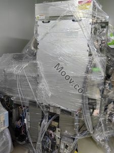


NIKON
NSR-S205C
CATEGORY
Steppers & Scanners
Last Verified: Over 60 days ago


Key Item Details
Condition:
Used
Operational Status:
Unknown
Product ID:
131673
Wafer Sizes:
4"/100mm, 6"/150mm, 8"/200mm, 12"/300mm
Vintage:
Unknown
Logistics Support
Available
Transaction Insured by Moov
Available
Refurbishment Services
Available
Description
Nikon KrF lithography machines use 248nm wavelength KrF excimer lasers as exposure light sources, which are suitable for more sophisticated semiconductor processes and are widely used in the manufacture of high-performance semiconductor devices, including microprocessors, dynamic random access memory (DRAM), and complex logic and mixed signal chips. These lithography machines are key equipment for achieving high-precision semiconductor device manufacturing, and play an important role in 4-inch, 6-inch, 8-inch and 12-inch wafer production lines, providing semiconductor manufacturers with flexibility and efficient production capabilities.Configuration
Scanning LSA:35 0.15 0.75 4:1 25*33 FIA:40OEM Model Description
This Nikon Step-and-Repeat Scanning System is compatible with both 200mm and 300mm process nodes and has a resolution of resolution ≦ 130 nm. When the NSR S205C was originally released in 2000, it boasted the the world's first ultra-high N.A. (0.75) projection lens as well as a KrF excimer laser. The system can process 140+ 200mm wafers/hour (16% higher throughput than Nikon's previous system). Applications for the NSR S205C include mass production of DRAM and MPU.Documents
No documents