


Description
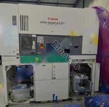
FPA-5000ES2+ (KrF)Configuration
No ConfigurationOEM Model Description
The FPA-5000ES2+ is a high-throughput 248-nanometer scanner for 0.15-micron ICs, introduced by Canon U.S.A. Inc.'s Semiconductor Equipment Division. It uses a 2-kilohertz, krypton-fluoride (KrF) excimer laser to expose 125 eight-inch wafers an hour and is aimed at a growing need for highly productive scanners with both 200- and 300-mm wafer capability. It has been designed to handle both 0.18- and 0.15-micron design rules, and allows field conversion from 200-mm to 300-mm wafer format within a day. It offers a 25% increase in throughput compared with its predecessor, the FPA-5000ES2.Documents
No documents

Verified
CATEGORY
Steppers & Scanners
Last Verified: Over 60 days ago
Key Item Details
Condition:
Used
Operational Status:
Unknown
Product ID:
109624
Wafer Sizes:
8"/200mm
Vintage:
Unknown
Logistics Support
Available
Transaction Insured by Moov
Available
Refurbishment Services
Available
Similar Listings
View All

CANON
FPA-5000ES2+
CATEGORY
Steppers & Scanners
Last Verified: Over 60 days ago


Key Item Details
Condition:
Used
Operational Status:
Unknown
Product ID:
109624
Wafer Sizes:
8"/200mm
Vintage:
Unknown
Logistics Support
Available
Transaction Insured by Moov
Available
Refurbishment Services
Available
Description
FPA-5000ES2+ (KrF)Configuration
No ConfigurationOEM Model Description
The FPA-5000ES2+ is a high-throughput 248-nanometer scanner for 0.15-micron ICs, introduced by Canon U.S.A. Inc.'s Semiconductor Equipment Division. It uses a 2-kilohertz, krypton-fluoride (KrF) excimer laser to expose 125 eight-inch wafers an hour and is aimed at a growing need for highly productive scanners with both 200- and 300-mm wafer capability. It has been designed to handle both 0.18- and 0.15-micron design rules, and allows field conversion from 200-mm to 300-mm wafer format within a day. It offers a 25% increase in throughput compared with its predecessor, the FPA-5000ES2.Documents
No documents