



Description
PLXD11 - Sistema de fotolitografia para exposição de lâminas de semicondutores cobertas com polímeros fotossensível usando luz ultravioleta e máscaras (retículos) para a fabricação de circuitos integrados eletrônicos -Configuration
No ConfigurationOEM Model Description
The PAS 5500/1100 193nm Step & Scan system enables 100nm mass production. The industry's leading resolution tool allows the current technology to be stretched to its limit. The PAS 5500/1100 combines the imaging power of the 0.75 NA 4x reduction lens with the AERIAL II ™ illumination technology. An array of advanced Illumination Enhancement technologies is optionally available. The system is equipped with ATHENA ™ and the newly developed RETICLE BLUE ALIGN providing an increased accuracy of single machine overlay of less than 20nm. A new level sensor improves focus and leveling particularly for edge die for better process control. Highly line narrowed 10W ArF lasers with Variable Laser Frequency Control in combination with the high optical transmission of the complete system provide a production throughput of 90 200mm wph with the lowest possible overall Cost of Operation. The PAS 5500/1100 system provides the highest value of ownership for leading-edge IC makers by combining a 0.75 numerical aperture (NA) lens, improved leveling performance and industry-leading overlay with an exposure capacity exceeding 90 200 mm wafers per hour at a dose of 20 mJ/cm2.Documents
No documents

Verified
CATEGORY
Steppers & Scanners
Last Verified: Over 60 days ago
Key Item Details
Condition:
Used
Operational Status:
Unknown
Product ID:
149293
Wafer Sizes:
Unknown
Vintage:
Unknown
Logistics Support
Available
Transaction Insured by Moov
Available
Refurbishment Services
Available
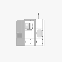
ASML
PAS 5500/1100
CATEGORY
Steppers & Scanners
Last Verified: Over 60 days ago


Key Item Details
Condition:
Used
Operational Status:
Unknown
Product ID:
149293
Wafer Sizes:
Unknown
Vintage:
Unknown
Logistics Support
Available
Transaction Insured by Moov
Available
Refurbishment Services
Available
Description
PLXD11 - Sistema de fotolitografia para exposição de lâminas de semicondutores cobertas com polímeros fotossensível usando luz ultravioleta e máscaras (retículos) para a fabricação de circuitos integrados eletrônicos -Configuration
No ConfigurationOEM Model Description
The PAS 5500/1100 193nm Step & Scan system enables 100nm mass production. The industry's leading resolution tool allows the current technology to be stretched to its limit. The PAS 5500/1100 combines the imaging power of the 0.75 NA 4x reduction lens with the AERIAL II ™ illumination technology. An array of advanced Illumination Enhancement technologies is optionally available. The system is equipped with ATHENA ™ and the newly developed RETICLE BLUE ALIGN providing an increased accuracy of single machine overlay of less than 20nm. A new level sensor improves focus and leveling particularly for edge die for better process control. Highly line narrowed 10W ArF lasers with Variable Laser Frequency Control in combination with the high optical transmission of the complete system provide a production throughput of 90 200mm wph with the lowest possible overall Cost of Operation. The PAS 5500/1100 system provides the highest value of ownership for leading-edge IC makers by combining a 0.75 numerical aperture (NA) lens, improved leveling performance and industry-leading overlay with an exposure capacity exceeding 90 200 mm wafers per hour at a dose of 20 mJ/cm2.Documents
No documents