RPM2000
Category
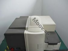
Photoluminescence MapperOverview
The RPM2000 is a Photoluminescence (PL) Mapping Tool designed specifically for the Compound Semiconductor market. It can handle substrate sizes of 75mm, 125mm, and 150mm and is used for detecting substrate defects and composition. Photoluminescence is a well-established, non-contact, non-destructive technique used in the development and process control of semiconductors. Room temperature PL wafer maps provide vital information on the uniformity of alloy composition, material quality, and defects in substrates, epilayers, and device structures. The RPM2000 has been designed to obtain whole wafer PL maps in a fraction of the time previously associated with this sort of measurement, giving the ability to measure and assess wafers between production runs. The primary benefit is that rapid feedback and remedial action can be implemented should wafer parameters be out of specification, avoiding wasted production runs thus saving time and costs. In addition, the speed of measurement also makes the incoming inspection and qualification of bought-in wafers a quick and easy task.
Active Listings
2
Services
Inspection, Insurance, Appraisal, Logistics