


Description
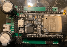
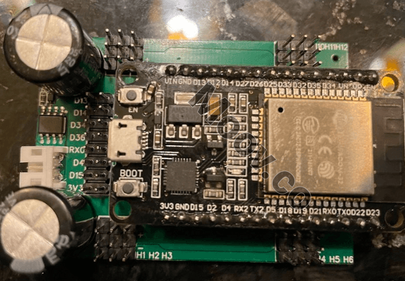
Supplier: Grande Layers:4 Application: ESS (Energy Storage Systems) Prototype PCB Assembly - Grande Electronics PCB:FR4/1.6mm/1oz Min Via: 0.2mm Surface Treatment: HASL PCBA Lead time: 3-4 weeks Testing: 100% E-test Standard Warp:<0.75% [Description] 1, Turnkey solution for ESS (Energy Storage Systems) Prototype PCB Assembly - Grande Electronics 2, PCB Assembly, PCB fabrication / PCB layout, PCB Reversing. 3, Full Bespoke PCBA/ OEM/ EMS(Electronics Manufacturing Services). 4, SMT&DIP&PTH&BGA. 5, Components Sourcing. 6, Quick PCBA prototype. 7, X-ray test, ICT and Functional Circuit Test. 8, Sample and small batch order are accepted. PCBA Service Customer offers: Gerber file, PCB Specification, BOM and Assembly Drawing. Full-turnkey PCBA: 1-30Layers PCB, Components Sourcing, SMT, PCBA testing, PCBA Aging test, PCBA Packing and PCBA Shipping. PCBA Quality Assurance 1, Certifications: UL, SGS, TUV, BV, ROHS, ISO9001: 2008, TS16949: 2008 2, 7 lines dust-proof SMT lines and DIP lines. 3, All line works wear anti-static and dust-proof clothing. 4, All operators should pass strictly training before they start work. 5, SMT Equipment:solder paste printer in Jidakang,, Mounter in Panasonic, Re-flow, Wave Soldering, Semi-auto DIP 6, PCBA Test Equipment: ORT, Constant temperature and humidity chamber,3D CMM,X-Ray. 7, PCBA Test:ICT, Functional Circuit Test and X-ray test. 8, Package Processed: 0402, 0603, 0805, 1206, 1608, 2125, 3216 Micro QFP 0.2mm Flip-chip, BGA, Connectors BGA Ball Pitch=0.2mm 9, Each workstation in accordance with the SOP 10, Materials:FR-4, FPC, Aluminum,High TG,Halogen-Free, HF, CEM-1, CEM-3, FR-1, 94-V0 and so on. 11, Material Brand:KB, SHENGYI, NANYA and so on. PCBA Lead Time PCBA prototype: 7-10 working days after contract signed and EQ confirmed. Mass production: partial delivery according to the customer’s requirement. Other information for PCBA 1, The mass production will be arranged after PCBA prototype confirmed. 2, Use Teflon adhesive tape to protect Mount Holes and GND Holes. 3, EPE is used to avoid impact and crash. PCBA Standard Packing Anti-static bag and compartmental packing https://www.grande-pcba.com/Configuration
ESS (Energy Storage Systems) Prototype PCB Assembly - Grande ElectronicsOEM Model Description
Type: Marking unit (controller + head) 13 W Standard area Marking method: XYZ 3-Axis simultaneous scanning method Marking laser Type: YVO4 laser, Class 4 Laser Product (IEC60825-1, JIS C6802, FDA [CDRH] part 1040.10)*1 Wavelength: 1,064 nm Output: 13 W Q-switch frequency: CW (continuous wave), 1 to 400 kHz Guide laser/Working distance pointer: Semiconductor laser, wavelength: 655 nm, output: 1.0 mW, Class 2 Laser Product (IEC60825-1, JIS C6802, FDA [CDRH] part 1040.10)*1 Marking area: 125 x 125 x 42 mm 4.92" x 4.92" x 1.65" Standard working distance (±variable width): 189 mm (±21 mm) 7.44" (±0.83") Marking resolution: 2 µm Scan speed: Max. 12,000 mm/s 472.44"/sDocuments
No documents


KEYENCE
MD-X1000
CATEGORY
Laser
Last Verified: Over 60 days ago

Key Item Details
Condition:
New
Operational Status:
Unknown
Product ID:
70542
Wafer Sizes:
2"/50mm
Vintage:
2319
Logistics Support
Available
Transaction Insured by Moov
Available
Refurbishment Services
Available
Description
Supplier: Grande Layers:4 Application: ESS (Energy Storage Systems) Prototype PCB Assembly - Grande Electronics PCB:FR4/1.6mm/1oz Min Via: 0.2mm Surface Treatment: HASL PCBA Lead time: 3-4 weeks Testing: 100% E-test Standard Warp:<0.75% [Description] 1, Turnkey solution for ESS (Energy Storage Systems) Prototype PCB Assembly - Grande Electronics 2, PCB Assembly, PCB fabrication / PCB layout, PCB Reversing. 3, Full Bespoke PCBA/ OEM/ EMS(Electronics Manufacturing Services). 4, SMT&DIP&PTH&BGA. 5, Components Sourcing. 6, Quick PCBA prototype. 7, X-ray test, ICT and Functional Circuit Test. 8, Sample and small batch order are accepted. PCBA Service Customer offers: Gerber file, PCB Specification, BOM and Assembly Drawing. Full-turnkey PCBA: 1-30Layers PCB, Components Sourcing, SMT, PCBA testing, PCBA Aging test, PCBA Packing and PCBA Shipping. PCBA Quality Assurance 1, Certifications: UL, SGS, TUV, BV, ROHS, ISO9001: 2008, TS16949: 2008 2, 7 lines dust-proof SMT lines and DIP lines. 3, All line works wear anti-static and dust-proof clothing. 4, All operators should pass strictly training before they start work. 5, SMT Equipment:solder paste printer in Jidakang,, Mounter in Panasonic, Re-flow, Wave Soldering, Semi-auto DIP 6, PCBA Test Equipment: ORT, Constant temperature and humidity chamber,3D CMM,X-Ray. 7, PCBA Test:ICT, Functional Circuit Test and X-ray test. 8, Package Processed: 0402, 0603, 0805, 1206, 1608, 2125, 3216 Micro QFP 0.2mm Flip-chip, BGA, Connectors BGA Ball Pitch=0.2mm 9, Each workstation in accordance with the SOP 10, Materials:FR-4, FPC, Aluminum,High TG,Halogen-Free, HF, CEM-1, CEM-3, FR-1, 94-V0 and so on. 11, Material Brand:KB, SHENGYI, NANYA and so on. PCBA Lead Time PCBA prototype: 7-10 working days after contract signed and EQ confirmed. Mass production: partial delivery according to the customer’s requirement. Other information for PCBA 1, The mass production will be arranged after PCBA prototype confirmed. 2, Use Teflon adhesive tape to protect Mount Holes and GND Holes. 3, EPE is used to avoid impact and crash. PCBA Standard Packing Anti-static bag and compartmental packing https://www.grande-pcba.com/Configuration
ESS (Energy Storage Systems) Prototype PCB Assembly - Grande ElectronicsOEM Model Description
Type: Marking unit (controller + head) 13 W Standard area Marking method: XYZ 3-Axis simultaneous scanning method Marking laser Type: YVO4 laser, Class 4 Laser Product (IEC60825-1, JIS C6802, FDA [CDRH] part 1040.10)*1 Wavelength: 1,064 nm Output: 13 W Q-switch frequency: CW (continuous wave), 1 to 400 kHz Guide laser/Working distance pointer: Semiconductor laser, wavelength: 655 nm, output: 1.0 mW, Class 2 Laser Product (IEC60825-1, JIS C6802, FDA [CDRH] part 1040.10)*1 Marking area: 125 x 125 x 42 mm 4.92" x 4.92" x 1.65" Standard working distance (±variable width): 189 mm (±21 mm) 7.44" (±0.83") Marking resolution: 2 µm Scan speed: Max. 12,000 mm/s 472.44"/sDocuments
No documents