


Description
No descriptionConfiguration
No ConfigurationOEM Model Description
AutoWafer is an ultrasonic wafer scanner for nondestructive testing (NDT) of wafers in development and production environments, providing high-resolution identification of bond defects in wafer applications such as MEMS, CMOS, memory, TSV and LED. Robotic cassette handling and sorting of approved and failed wafers helps speed production, while our advanced transducers and auto-analysis tools make it quick and easy to identify even the smallest, most subtle defects. -The ideal automatic ultrasonic testing system for detecting wafer-to-wafer bonding defects -A fully automated, production-ready wafer scanner for MEMS, CMOS, BSI sensors, memory, TSV, LED and other applications employing wafers 200mm and smaller -Provides wafer map with die-level pass/fail indicators (optional) -Provides analysis (optional) -200mm SECS/GEM -TSV entrenched metrologyDocuments
No documents

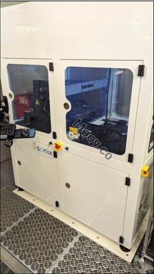
SONIX
AutoWafer
CATEGORY
Defect Inspection
Last Verified: Over 60 days ago


Key Item Details
Condition:
Used
Operational Status:
Unknown
Product ID:
72971
Wafer Sizes:
Unknown
Vintage:
Unknown
Logistics Support
Available
Transaction Insured by Moov
Available
Refurbishment Services
Available
Description
No descriptionConfiguration
No ConfigurationOEM Model Description
AutoWafer is an ultrasonic wafer scanner for nondestructive testing (NDT) of wafers in development and production environments, providing high-resolution identification of bond defects in wafer applications such as MEMS, CMOS, memory, TSV and LED. Robotic cassette handling and sorting of approved and failed wafers helps speed production, while our advanced transducers and auto-analysis tools make it quick and easy to identify even the smallest, most subtle defects. -The ideal automatic ultrasonic testing system for detecting wafer-to-wafer bonding defects -A fully automated, production-ready wafer scanner for MEMS, CMOS, BSI sensors, memory, TSV, LED and other applications employing wafers 200mm and smaller -Provides wafer map with die-level pass/fail indicators (optional) -Provides analysis (optional) -200mm SECS/GEM -TSV entrenched metrologyDocuments
No documents